Paste Area Ratio Calculator
Sometimes if a solder stencil aperture is too small (relative to the stencil thickness) the paste will remain in the stencil when it's lifted off the PCB. This is because the paste's adhesion to the stencil is higher than it's adhesion to the PCB. Since paste adhesion to a surface is proportional to the surface area contacting that surface, the area ratio of the stencil opening can help you determine if this is likely to happen.
The area ratio is the ratio of the surface area of the paste that's against the stencil to the area that's against the PCB. Therefore, it's equation is:
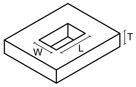
$$\text{Area Ratio} = \frac{ \text{Area of Aperature Opening} }{ \text{Area of Aperature Walls} } = \frac{L*W}{2(L+W)*T}$$Where L, W, and T and defined in the below figure:
Below you can quickly calculate the area ratio:
Stencil Thickness: milPad Length: mm
Pad Width: mm
Area Ratio:
Top Google Results for Area Ratio Guidelines
Macaos: "This ratio should be at least 0.66."
QualiEco Circuits "The generally accepted design guideline for acceptable paste release is [greater than] 0.66 for the area ratio..."
Indium Corp "A rule of thumb that still seems to hold is that the area ratio should be 0.66 or greater for the best printing result."
Without a more authoritative source, the best I can say is that people seem to agree that the area ratio should be at least 0.66 to give good release results.
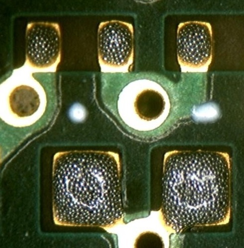
Solder paste applied to a PCB using a stencil.
Image courtesy of Wikipedia,
CC BY-SA 3.0